How Can You Master Solder Pallet Design for Flawless Soldering?
Written By Loris Chow
You’ve chosen the perfect material, but your soldering results are still inconsistent. The problem often lies not in the material itself, but in the blueprint used to shape it.
A comprehensive solder pallet design guide involves mastering four areas: selecting the correct material thickness, implementing effective hold-downs, designing precise masking walls, and ensuring compatibility with your conveyor system. This blueprint is the key to flawless support and soldering outcomes.

I’ll never forget a high-stakes project involving a dense server board. We had a pallet made from what we thought was a premium Durostone material, but we kept seeing random solder skips. After days of troubleshooting, we discovered the masking wall was a millimeter too tall and too close to a row of pins. It was creating a "solder shadow." That day, I learned that a great material is only as good as its design. Mastering the blueprint is not optional; it’s essential for extending solder pallet life and guaranteeing quality.
Is Your Pallet’s Thickness a Compromise Between Strength and Performance?
Choosing pallet thickness seems simple—thicker is stronger, right? But this decision is a critical balancing act that directly impacts both the pallet’s durability and the quality of your soldering.
Yes, pallet thickness is a crucial compromise. It must be thick enough to resist warping under thermal stress but thin enough to minimize heat absorption, which could negatively affect the PCB’s thermal profile and slow down the production line.

Dive Deeper: The Thermal and Mechanical Trade-Off
The core function of a solder pallet is to remain perfectly flat through extreme temperature changes. A thicker pallet (8-12mm) offers superior strength, which is critical for preventing solder pallet warping issues, especially with large, heavy boards. However, this robustness comes at a thermal cost. The pallet acts as a heat sink, and a thicker design absorbs more energy, potentially pulling heat away from the PCB and slowing down cycle times. This is also where the challenge of machining solder pallet materials comes into play; a thicker block requires more machining time and can be tougher on cutting tools.
Conversely, a thinner pallet (5-6mm) is more thermally efficient but far more susceptible to warping over time. The ideal thickness is a calculated choice based on your specific application, balancing the need for mechanical rigidity with thermal performance.
| Pallet Thickness | Advantages | Disadvantages | Best Use Case |
|---|---|---|---|
| Thick (8-12mm) | High rigidity, excellent warp resistance, long life. | High thermal mass, can alter thermal profile, longer cycle time. | Large, heavy PCBs; high-volume production. |
| Thin (5-6mm) | Low thermal mass, minimal process impact, fast cycle time. | Lower rigidity, more prone to warping over time. | Small, lightweight PCBs; prototyping. |
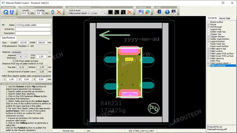
How Do You Design Masking Walls That Protect Without Causing Defects?
The primary job of a pallet wall is to shield components. But what happens when the shield itself creates a new problem by blocking the very solder it’s supposed to control?
Effective wall design requires balancing height and proximity. The wall must be tall enough to block solder but positioned far enough from through-hole joints to prevent "solder shadowing," an effect where the wall obstructs solder flow and causes skips.

Dive Deeper: Avoiding the Solder Shadow Effect
The "solder shadow" is one of the most common pallet-induced defects. It occurs when a masking wall is too close to a Plated-Through-Hole (PTH) that needs to be soldered, disrupting the flow of the molten solder and causing an incomplete joint. The solution lies in careful geometric design, a core part of any solder pallet design guide.
A general rule is that the distance from the wall to the joint should be at least two to three times the wall’s height. When space is tight, advanced design techniques are necessary. This can involve tapered or chamfered walls, which requires precision machining solder pallet materials like Ricocel or Durostone. The ability to create these fine features without chipping or cracking is a testament to both the material quality and the skill of the machinist. For extremely dense boards, designers might create complex, multi-level pockets to provide protection without casting a large shadow, turning the pallet into a truly engineered tool.
| Design Challenge | Poor Design Choice | Better Design Solution | Rationale |
|---|---|---|---|
| Dense Components | A tall, vertical wall placed very close to a PTH pin. | Taper the wall, or use a stepped design. | Reduces the "shadow" profile while still providing protection. |
| Protecting a Connector | One large pocket around the entire connector. | Individual masking around pin groups, with channels for solder flow. | Allows solder to reach all necessary joints without obstruction. |
| Fine-Pitch PTH | Standard thickness walls between all pins. | Use knife-edge thin walls or selective masking only where needed. | Minimizes total obstruction in a dense area. |
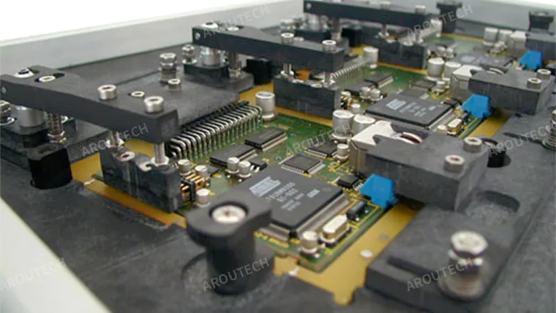
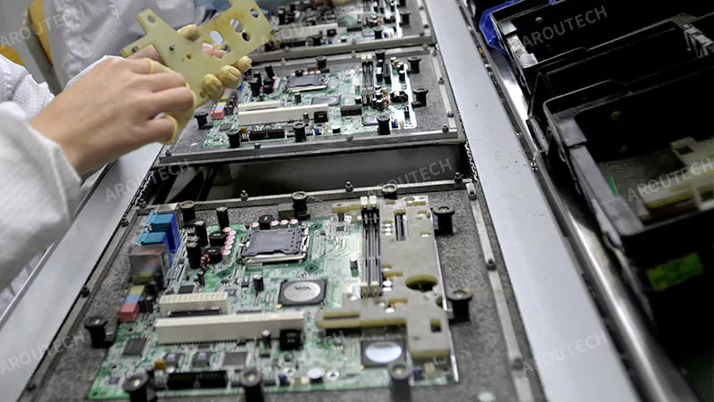
What Type of Hold-Down is Right for Your PCB?
Simply placing a PCB in a pallet pocket isn’t enough; it needs to be actively secured to prevent movement and warping during the intense heat of the soldering process.
The right hold-down depends on the PCB’s characteristics. Spring-loaded clamps are ideal for thin, flexible boards that need downward pressure, while simple rotating clamps are robust and effective for securing standard, rigid boards.

Dive Deeper: A Guide to Securing Your Assembly
Hold-downs are the active components of a solder pallet, and their primary job is to prevent the PCB from lifting or bowing. An unsecured board can warp, leading to catastrophic soldering failures and contributing to what operators might mistake for solder pallet warping issues. The choice of mechanism is a key design decision.
- Rotating Clamps: These are the simplest and most common. They are small clamps, often machined from the same pallet material for thermal compatibility, that rotate to secure the board edge. They are robust and have no metal parts to fail.
- Spring-Loaded Hold-Downs: Essential for thin or flexible PCBs. A small spring applies constant downward pressure, forcing the board to stay flat.
- Push-Pull Clamps: Specialized metal clamps offering very strong force, often used for large, heavy boards.
- Integrated Flexible Tabs: For some applications, small, flexible tabs can be machined directly into the pallet wall, offering a low-cost solution for light-duty applications.
The design must also be ergonomic. Hold-downs should be easy for an operator to engage and disengage quickly and safely, a crucial factor in maintaining production line speed.
Conclusion
Mastering this solder pallet design guide transforms a simple carrier into a precision instrument. By carefully engineering every detail—from thickness and wall design to the specific type of hold-down—you build the blueprint for a stable, high-yield, and flawless soldering process.
References
- Solder Pallet: Wikipedia contributors. "Solder pallet." Wikipedia, The Free Encyclopedia.
- Computer-Aided Design (CAD): Wikipedia contributors. "Computer-aided design." Wikipedia, The Free Encyclopedia.
- CNC Machining: CNC Cookbook. "CNC Machining: An Introduction."
- Printed Circuit Board (PCB): Wikipedia contributors. "Printed circuit board." Wikipedia, The Free Encyclopedia.
- Plated-Through-Hole (PTH): Wikipedia contributors. "Through-hole technology." Wikipedia, The Free Encyclopedia.
Latest insights & related news
What is a Wave Solder Pallet and Why is it Critical for Your PCBA Production?
Are you struggling with inconsistent soldering, high defect rates, and production bottlenecks? You’ve optimized your process, but the root cause might be an overlooked, yet essential, tool. A wave solder pallet is a custom-machined carrier, typically made from a high-performance composite solder pallet material, that precisely holds, masks, and protects a Printed Circuit Board Assembly […]
How Can You Master Solder Pallet Design for Flawless Soldering?
You’ve chosen the perfect material, but your soldering results are still inconsistent. The problem often lies not in the material itself, but in the blueprint used to shape it. A comprehensive solder pallet design guide involves mastering four areas: selecting the correct material thickness, implementing effective hold-downs, designing precise masking walls, and ensuring compatibility with […]
How Do You Choose the Right Solder Pallet Material for Your Process?
You know what a solder pallet is and why it’s critical. But now you face the core decision: choosing the material. Pick the wrong one, and you could face warping, chemical damage, and a short pallet lifespan, undermining your entire investment. To choose the right solder pallet material, you must conduct a solder pallet material […]