What is a Wave Solder Pallet and Why is it Critical for Your PCBA Production?
Written By Loris Chow
Are you struggling with inconsistent soldering, high defect rates, and production bottlenecks? You’ve optimized your process, but the root cause might be an overlooked, yet essential, tool.
A wave solder pallet is a custom-machined carrier, typically made from a high-performance composite solder pallet material, that precisely holds, masks, and protects a Printed Circuit Board Assembly (PCBA) during the wave soldering process. It is absolutely critical for achieving high quality, repeatability, and efficiency in modern electronics manufacturing.

I remember an early project in my career involving a complex motherboard with components on both sides. Our initial attempts to wave solder it without a proper fixture were a complete disaster. We faced constant board warping, and solder was getting everywhere it shouldn’t. The production line was halted, and pressure was mounting. It was only when we invested in a custom-designed solder pallet, made from a proper lead-free solder pallet material, that everything clicked into place. Suddenly, our process was stable, and our yield shot up. That experience taught me a vital lesson: a solder pallet isn’t just an accessory; it’s the foundation upon which a reliable soldering process is built.
How Does a Solder Pallet Guarantee Perfect Alignment?
Think a PCB just sits flat on the conveyor? In reality, even slight misalignments can lead to disastrous soldering defects, turning a high-value assembly into scrap in seconds.
A wave solder pallet acts like a custom-fit glove, using precisely machined pockets and locating pins to lock the PCB into an exact, repeatable position. This guarantees perfect alignment with the solder wave every single time, eliminating a major source of process variation.

Dive Deeper: The Engineering of Precision
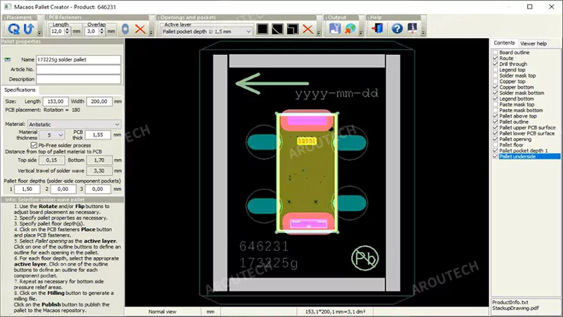
The concept of precise positioning goes beyond simply holding the board. It’s about creating a perfect, unchangeable relationship between the Printed Circuit Board (PCB) [1, 2, 3] and the wave soldering machine. The design of a pallet starts with the board’s digital blueprint, the Gerber files [1, 2]. The pallet is then machined to tolerances often measured in micrometers to create a snug pocket for the PCB. This level of precision is only possible because the chosen solder pallet material is dimensionally stable and does not expand or contract significantly during thermal cycling. This stability ensures the board cannot shift or vibrate as it moves along the conveyor. It also establishes a consistent Z-axis height, ensuring the bottom of the board maintains the optimal distance from the crest of the solder wave. By locking the PCB into a fixed, known position, the pallet removes these variables, making the process highly repeatable.
| Positioning Feature | Function | Impact on Quality |
|---|---|---|
| Machined Pocket | Conforms to the PCB’s exact outline. | Prevents horizontal shifting and rotation. |
| Locating Pins | Engage with tooling holes on the PCB. | Provides the primary, non-negotiable registration point. |
| Edge Rails | Ensure smooth, stable movement on the conveyor. | Prevents vibration and inconsistent travel speed. |
Why is Selective Masking the Pallet’s Most Powerful Feature?
Modern PCBs are densely packed with components on both sides. How can you possibly pass the bottom side through a wave of molten solder without destroying everything?
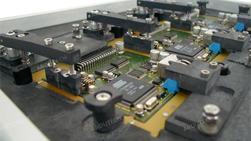
Selective masking is the pallet’s superpower. It creates a physical barrier that selectively exposes only the through-hole leads that need soldering, while shielding all other sensitive areas like SMT components, connectors, and gold fingers from the heat and solder.

Dive Deeper: The Art of Shielding
The rise of mixed-technology boards makes selective masking essential. The excellent machinability of modern composite solder pallet materials allows for the creation of intricate pockets and "solder dams" on the pallet’s underside. These features are meticulously designed to cover and protect every sensitive area, from tiny Surface-Mount Technology (SMT) [1, 2] components to complex Ball Grid Arrays (BGAs) [1, 2]. The walls of these pockets must be tall enough to prevent solder from splashing over, yet thin enough to not create a "shadowing" effect that would block solder from reaching nearby PTH joints. A well-designed pallet effectively makes a complex, double-sided board appear as a simple, single-sided board to the wave solder machine, enabling a process that would otherwise be impossible.
| Positioning Feature | Function | Impact on Quality |
|---|---|---|
| Machined Pocket | Conforms to the PCB’s exact outline. | Prevents horizontal shifting and rotation. |
| Locating Pins | Engage with tooling holes on the PCB. | Provides the primary, non-negotiable registration point. |
| Edge Rails | Ensure smooth, stable movement on the conveyor. | Prevents vibration and inconsistent travel speed. |
Can a Simple Pallet Really Prevent Costly PCB Warping?
PCBs are thin, and the wave soldering process is intensely hot. This combination is a perfect recipe for PCB deformation, a defect that can cause a cascade of other problems.
Yes, absolutely. The pallet provides a rigid, flat backbone for the PCB throughout the entire thermal cycle. This structural support, derived from the right wave solder pallet material, is critical for preventing the board from sagging or twisting when heated.

Dive Deeper: Defeating Thermal Deformation
The most common material for PCBs is FR-4, which softens significantly when it approaches its Glass Transition Temperature (Tg) [1, 2]. This is where solder pallet warping issues often begin. Without support, a thin PCB will inevitably sag in the heat of the soldering machine. This is why the choice of solder pallet material is so critical. The pallet itself is made from a specialized composite, such as Durostone material or Ricocel material, engineered to have a much higher Tg and superior thermal stability. This high-temperature resistance pallet material acts as a rigid backbone, holding the PCB perfectly planar. It provides uniform support across the entire board surface, often supplemented by special hold-downs. This ensures that every part of the board is presented to the solder wave at the exact same height and angle, guaranteeing a consistent and reliable soldering result.
How Can Solder Pallets Dramatically Increase Your Throughput?
In manufacturing, time is money. Processing one board at a time, especially if they are small or irregularly shaped, creates a major bottleneck that slows down your entire production line.
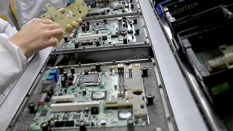
Solder pallets are a massive efficiency multiplier. They allow you to combine multiple smaller boards into a single large panel (panelization), or to handle oddly shaped boards using a standardized carrier, dramatically increasing throughput and simplifying machine setup.

Dive Deeper: The Power of Panelization and Standardization
Imagine your product is a small PCB. Processing these one by one is incredibly inefficient. A solder pallet can be designed to hold a panel of these boards, for instance, a 4×4 array of 16 boards. Now, with a single pass through the wave solder machine, you have processed 16 units instead of one. This strategy, known as panelization, is one of the most effective ways to reduce cycle time. Furthermore, modern composite solder pallet materials offer an excellent strength-to-weight ratio, making even large, panelized pallets manageable for operators. Many are also available as an anti-static pallet material to protect sensitive electronic components from electrostatic discharge (ESD) during handling, adding another layer of process security. This standardization simplifies operator tasks and reduces setup time, leading to a more streamlined and efficient production flow.
Conclusion
A wave solder pallet is far more than a simple holder. It is a precision-engineered tool that provides the four pillars of successful wave soldering. These functions are only made possible by the advanced solder pallet materials used in their construction. Understanding these functions is the first step, and knowing how to choose solder pallet material—a topic we will explore next—is the key to unlocking maximum performance.
References
- Wave Soldering: Wikipedia contributors. "Wave soldering." Wikipedia, The Free Encyclopedia.
- Solder Pallet: Wikipedia contributors. "Solder pallet." Wikipedia, The Free Encyclopedia.
- Printed Circuit Board (PCB): Wikipedia contributors. "Printed circuit board." Wikipedia, The Free Encyclopedia.
- Printed Circuit Board Assembly (PCBA): Circuit Assembly. "What is a PCBA (Printed Circuit Board Assembly)?"
- Surface-Mount Technology (SMT): Wikipedia contributors. "Surface-mount technology." Wikipedia, The Free Encyclopedia.
- Ball Grid Array (BGA): Wikipedia contributors. "Ball grid array." Wikipedia, The Free Encyclopedia.
- Gerber File: Wikipedia contributors. "Gerber format." Wikipedia, The Free Encyclopedia.
- Glass Transition Temperature (Tg): Wikipedia contributors. "Glass transition." Wikipedia, The Free Encyclopedia.
Latest insights & related news
What is a Wave Solder Pallet and Why is it Critical for Your PCBA Production?
Are you struggling with inconsistent soldering, high defect rates, and production bottlenecks? You’ve optimized your process, but the root cause might be an overlooked, yet essential, tool. A wave solder pallet is a custom-machined carrier, typically made from a high-performance composite solder pallet material, that precisely holds, masks, and protects a Printed Circuit Board Assembly […]
How Can You Master Solder Pallet Design for Flawless Soldering?
You’ve chosen the perfect material, but your soldering results are still inconsistent. The problem often lies not in the material itself, but in the blueprint used to shape it. A comprehensive solder pallet design guide involves mastering four areas: selecting the correct material thickness, implementing effective hold-downs, designing precise masking walls, and ensuring compatibility with […]
How Do You Choose the Right Solder Pallet Material for Your Process?
You know what a solder pallet is and why it’s critical. But now you face the core decision: choosing the material. Pick the wrong one, and you could face warping, chemical damage, and a short pallet lifespan, undermining your entire investment. To choose the right solder pallet material, you must conduct a solder pallet material […]