Layout of components on SMT-PCB
-
When a circuit board is put into the reflow soldering furnace of the conveyor belt, the components of the long axis should be vertical in the equipment of transmission direction, so that we can prevent the occurrence of drift during the welding process, or monuments of “vertical” phenomenon.
-
The components of the PCB should be evenly distributed. In particular, the high-power devices should be dispersed to avoid any local overheating of the PCB when the circuit is working. Overheating will affect the reliability of the solder points.
-
The application of the double-sided pasted components shall be staggered and installed on both sides, otherwise, the welding effect will be affected by the increase of local heat capacity during the welding process.
-
The PLCC/QFP device cannot be placed on the welding face of wave peak.
-
The SMT large device installed on the welding surface of the wave peak shall be parallel to the direction of the solder wave peak flow, so as to reduce the welding between electrodes.
-
SMT components, both large and small on the surface of the wave soldering, cannot be arranged in a straight line. You must stagger their position, so as to protect the welding with the solder wave “shadow” effect of virtual welding and leakage caused by the welding.
Welding disks on SMT-PCB
-
Wave soldering SMT components to the surface of the bonding pad of the larger components, such as transistors, socket, etc., to the appropriate increase, such as the bonding pad of SOT23, can be lengthened 0.81 mm, so that we can avoid the element of “shadow effect” and the empty welding.
-
The size of the welding disk shall be determined according to the dimensions of the components. The width of the welding disk is equal to or slightly larger than the width of the electrode of the component for the best welding effect.
-
Between the two connected components, avoid big welding using a single disk, because big welding plate solder will take two components to the middle. The correct thing to do is to separate the two components of the bonding pad, go between the two bonding pads with a finer wire connection, and possible have parallel wires through the larger current several wires, and cover green oil on the wire.
-
SMT components of the bonding pad on or near the hole, otherwise, in the process of REFLOW solder on the pads will flow down the hole after melting, which will produce virtual welding, little tin, and is also likely to cause a short circuit flow to the other side of the board.
Latest insights & related news
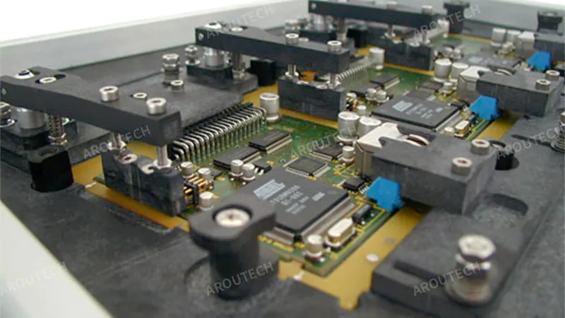
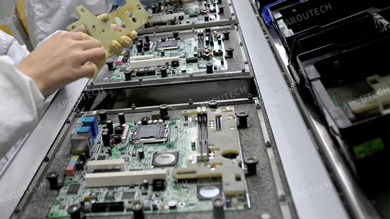
What is a Wave Solder Pallet and Why is it Critical for Your PCBA Production?
Are you struggling with inconsistent soldering, high defect rates, and production bottlenecks? You’ve optimized your process, but the root cause might be an overlooked, yet essential, tool. A wave solder pallet is a custom-machined carrier, typically made from a high-performance composite solder pallet material, that precisely holds, masks, and protects a Printed Circuit Board Assembly […]
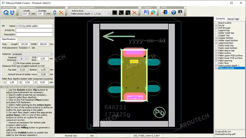
How Can You Master Solder Pallet Design for Flawless Soldering?
You’ve chosen the perfect material, but your soldering results are still inconsistent. The problem often lies not in the material itself, but in the blueprint used to shape it. A comprehensive solder pallet design guide involves mastering four areas: selecting the correct material thickness, implementing effective hold-downs, designing precise masking walls, and ensuring compatibility with […]
How Do You Choose the Right Solder Pallet Material for Your Process?
You know what a solder pallet is and why it’s critical. But now you face the core decision: choosing the material. Pick the wrong one, and you could face warping, chemical damage, and a short pallet lifespan, undermining your entire investment. To choose the right solder pallet material, you must conduct a solder pallet material […]